


SN74HC595N Shift Register: Led Pinout, Features, and Datasheet
 383
383Global electronic component supplier ERSAELECTRONICS: Rich inventory for one-stop shopping. Inquire easily, and receive fast, customized solutions and quotes.
SN74HC595N Led Pinout
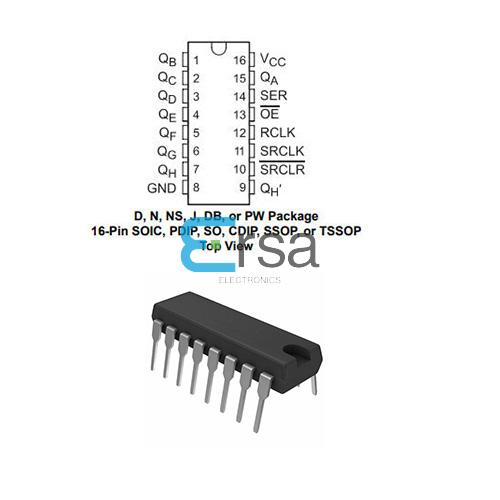
| Pin No. | Pin Name | Description | Function in LED Control |
| 1 | Q1 | Output pin 1 (parallel output) | Connect to LED 1's cathode or anode depending on the circuit configuration. |
| 2 | Q2 | Output pin 2 (parallel output) | Connect to LED 2. |
| 3 | Q3 | Output pin 3 (parallel output) | Connect to LED 3. |
| 4 | Q4 | Output pin 4 (parallel output) | Connect to LED 4. |
| 5 | Q5 | Output pin 5 (parallel output) | Connect to LED 5. |
| 6 | Q6 | Output pin 6 (parallel output) | Connect to LED 6. |
| 7 | Q7 | Output pin 7 (parallel output) | Connect to LED 7. |
| 8 | GND | Ground pin | Connect to the ground of the power supply. |
| 9 | Q7' (Serial Out) | Serial data output for daisy-chaining to another shift register | Used for chaining another SN74HC595N if more outputs are needed. |
| 10 | MR (Master Reset) | Active-low reset pin that clears the shift register | Pulled HIGH or connected to the reset circuit, resets all outputs to LOW when activated. |
| 11 | SH_CP (Shift Clock) | Clock pin that shifts the serial data through the register on the rising edge | Connect to the microcontroller's clock pin to synchronize data shifting for the LEDs. |
| 12 | ST_CP (Storage Clock/Latch) | Latches the data from the shift register to the output register on the rising edge | Connect to a clock pin to latch the output data, updating the LEDs based on the shifted data. |
| 13 | OE (Output Enable, Active LOW) | Enables or disables the outputs, low = enable, high = disable | Connect to ground for always-on output, or to a control pin for output enable/disable control. |
| 14 | DS (Serial Data Input) | Serial data input for the shift register | Connect to the microcontroller's data pin for feeding data to control the LEDs. |
| 15 | Q0 | Output pin 0 (parallel output) | Connect to LED 0. |
| 16 | VCC | Power supply (2V-6V) | Connect to the positive terminal of the power supply. |
SN74HC595N CAD Model
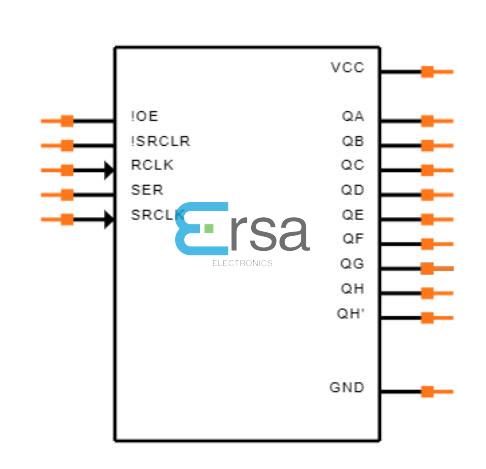
Figure 1: SN74HC595N Symbol
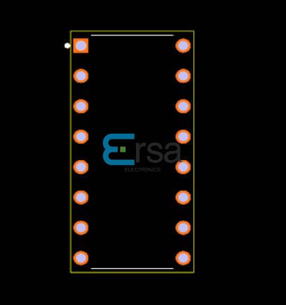
Figure 2: SN74HC595N Footprint
What is an SN74HC595N Shift Register?
The SN74HC595N shift register is essential in applications where additional output pins are required from a microcontroller, without increasing the pin count. It efficiently converts serial data into parallel outputs, enabling the control of multiple devices such as LEDs, relays, or displays.
The SN74HC595N operates across a voltage range of 2V to 6V, making it suitable for various low-voltage and standard-voltage applications. Its low power consumption of just 80 μA ensures minimal energy usage, making it an excellent choice for power-sensitive designs.
Another advantage of this IC is its daisy-chaining capability. By connecting multiple SN74HC595N chips in series, users can control more outputs with the same number of microcontroller pins, simplifying complex designs while optimizing pin usage. This scalability makes the IC highly adaptable for projects requiring expandable outputs, such as multiplexed LED displays, driving multiple motors, or controlling large arrays of sensors.
Key Features of SN74HC595N
The SN74HC595N is an 8-bit serial-in, parallel-out shift register from Texas Instruments, widely used in digital circuits for expanding I/O capabilities. Here are its key features:
1. Data Handling:
8-Bit Serial-In, Parallel-Out Shift Register: The device accepts data serially and outputs it in parallel, making it efficient for applications requiring multiple outputs from a single microcontroller pin.
2. Voltage and Power Specifications:
Wide Operating Voltage Range: It operates between 2 V and 6 V, allowing flexibility in different electronic applications.
Low Power Consumption: The maximum supply current (ICC) is 80 µA, making it suitable for battery-powered devices.
3. Output Characteristics:
High-Current 3-State Outputs: Capable of driving up to 15 LSTTL loads, which is beneficial for interfacing with various components like LEDs or other digital devices.
Output Drive Capability: Provides a drive of ±6 mA at 5 V, ensuring sufficient current for connected loads.
4. Timing and Performance:
Typical Propagation Delay (tpd): Approximately 13 ns, allowing for fast operation in high-speed applications.
Low Input Current: The maximum input current is only 1 µA, which helps in reducing power consumption further.
5. Functional Features:
Direct Clear Functionality: The shift register includes a direct overriding clear (SRCLR) input, enabling immediate reset of the output state.
Cascading Capability: Multiple SN74HC595N devices can be daisy-chained to expand the number of outputs, making it scalable for larger projects.
SN74HC595N Specifications
| Specification of SN74HC595N | Details |
| Part Number | SN74HC595N |
| Function | 8-bit Serial-In, Parallel-Out (SIPO) Shift Register with Latch |
| Number of Outputs | 8 parallel outputs (Q0 to Q7) |
| Voltage Supply Range | 2V to 6V |
| Maximum Clock Frequency | 100 MHz |
| Output Current | ±6 mA per output at 5V |
| Low Power Consumption | 80 µA (max) |
| Operating Temperature | -40°C to +85°C |
| Propagation Delay | 16 ns (typical) at 5V |
| Logic Type | CMOS |
| Reset | Active-Low Master Reset (MR) |
| Output Enable | Active-Low Output Enable (OE) |
| Data Input | Serial Data Input (DS) |
| Clock Inputs | Shift Clock (SH_CP) and Storage Clock/Latch (ST_CP) |
| Daisy-Chaining | Yes (via Q7' serial output) |
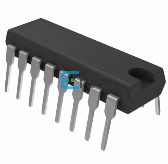
| Package Type | DIP-16 (Dual Inline Package, 16 pins) |
| Quiescent Current | 2 µA (max) |
| Pin Count | 16 pins |
| Latch Function | Data is latched to outputs on the rising edge of the storage clock (ST_CP) |
| 3-State Outputs | Outputs can be HIGH, LOW, or high-impedance |
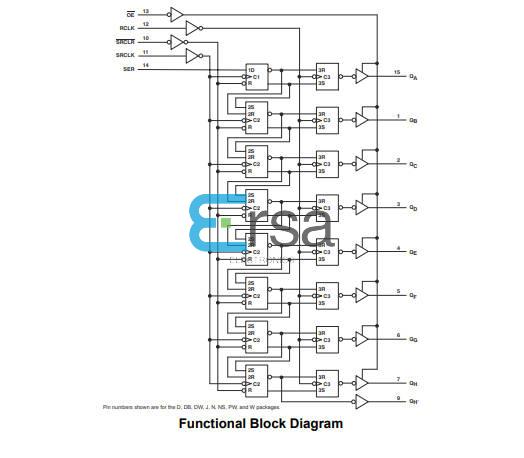
SN74HC595N Block Diagram
Advantages of Using SN74HC595N
Data Handling Efficiency:
The SN74HC595N converts serial data into parallel outputs, allowing for the control of multiple devices using fewer microcontroller pins. This is particularly beneficial in applications where pin availability is limited, such as with Arduino microcontrollers.
High Speed:
This shift register features a significantly lower propagation delay of only 13 nanoseconds, compared to its predecessors. This allows for faster data processing and reduces the risk of delays accumulating in high-speed applications.
Daisy Chaining Capability:
Multiple SN74HC595N chips can be daisy-chained together, increasing the number of outputs without requiring additional control lines. This scalability is advantageous for projects needing to manage numerous outputs, such as LED displays or sensor arrays.
Low Power Consumption:
Operating at a voltage range of 2V to 6V, the SN74HC595N consumes minimal power (approximately 80 µA), making it suitable for battery-powered devices or energy-efficient designs.
Versatile Applications:
The SN74HC595N is widely used in various applications including LED driving, digital displays, and control systems for home automation. Its ability to handle both serial and parallel data makes it adaptable for numerous electronic projects.
Noise Immunity:
Designed with high noise immunity, the SN74HC595N can operate reliably in environments with electrical interference, which is crucial for maintaining signal integrity in complex circuits.
Simple Design and Implementation:
The straightforward pin configuration and operation make it easy to integrate into existing designs. Its functionality can be easily controlled through basic programming, simplifying development efforts for engineers and hobbyists alike.
Cost-Effectiveness:
The SN74HC595N provides a low-cost solution for expanding output capabilities without the need for additional microcontrollers or complex circuitry.
In summary, the SN74HC595N shift register is a highly efficient and versatile component that enhances the capabilities of microcontroller-based systems by enabling high-speed data handling, scalability through daisy chaining, and low power consumption while maintaining reliability in various applications.
SN74HC595N Compared to Other Shift Registers
| Feature | SN74HC595N | 74HC164 | 74HCT595 |
| Functionality | Has a storage register that maintains stable output during data shifts, preventing flicker. | Outputs are directly tied to flip-flop states, leading to possible temporary errors. | Includes a storage register but with slower performance than SN74HC595N. |
| Output Control | Features an output enable (OE) pin for high-impedance state control. | Lacks an OE pin, and only has a clear terminal. | Similar to SN74HC595N, supports three-state output control. |
| Daisy-Chaining Capability | Supports daisy-chaining for expanding outputs with minimal microcontroller pins. | Does not support efficient daisy-chaining. | Supports daisy-chaining but with slower propagation. |
| Drive Current | It can drive up to 35mA per output. | Limited to 25mA per output. | Similar to SN74HC595N, can handle moderate currents. |
| Propagation Delay | Fast propagation delay (~13 ns). | Not applicable, as it’s not designed for high-speed applications. | Slower with ~240 ns propagation delay, limiting its use in high-speed circuits. |
| Voltage Range | Operates between 2V and 6V. | Similar voltage range. | Operates in a narrower range of 4.5V to 5.5V, reducing flexibility. |
| Three-State Output | Supports three-state outputs, ideal for bus sharing in complex systems. | Does not have a three-state output capability. | Similar three-state output functionality to SN74HC595N. |
| Internal Architecture | Separate clocks for shift register and storage register, providing precise data control. | Single clock, which may lead to less precise data handling. | Similar architecture, but is slower than SN74HC595N. |
The SN74HC595N stands out due to its advanced features such as a storage register, higher drive current capabilities, faster propagation delay, and enhanced output control options. These attributes make it more suitable for complex applications requiring reliable data handling and output management compared to alternatives like the 74HC164 and 74HCT595.
SN74HC595N Equivalents
| SN74HC595N Equivalents | Manufacturer | Description | Key Differences/Similarities |
| 74HC595 | Various (e.g., NXP, STMicroelectronics) | 8-bit shift register with output latches and 3-state outputs. | Direct equivalent, typically the same specifications as SN74HC595N. |
| 74HCT595 | Texas Instruments | High-speed 8-bit shift register, TTL-compatible input levels. | Similar, but slower propagation delay (240 ns) and works better in TTL-level systems. |
| M74HC595 | STMicroelectronics | 8-bit serial-in, parallel-out shift register. | Same functionality as SN74HC595N, different manufacturer. |
| CD4094 | Texas Instruments | 8-stage shift-and-store register with output latches. | Similar functionality but operates at lower speeds and different voltage ranges (3V to 15V). |
| TPIC6B595 | Texas Instruments | Power logic 8-bit shift register with high-current outputs. | Higher current capability (up to 150mA per output), ideal for driving power-hungry devices. |
| HEF4094 | NXP Semiconductors | 8-stage shift-and-store register. | Similar to SN74HC595N but with slower speed and operates over a wider voltage range. |
| MC14094B | ON Semiconductor | 8-stage static shift register with storage latches. | Similar functionality but slower and with a broader voltage range (3V to 18V). |
The SN74HC595N has several equivalents, including the 74HC595, which is a direct replacement with identical functionality. Other parts like the 74HCT595 and CD4094 offer similar functionality but differ in speed, voltage range, or drive capability. For higher power applications, the TPIC6B595 can be used, while options like the HEF4094 and MC14094B provide similar features but with wider operating voltage ranges and slower performance. These alternatives offer flexibility based on the specific needs of a circuit, such as speed, current handling, or voltage range.
SN74HC595N Applications
LED Control:
- The SN74HC595N is commonly used to drive multiple LEDs, allowing for intricate lighting patterns and effects in projects such as light displays and decorative lighting setups. Its ability to manage numerous outputs while using minimal GPIO pins makes it ideal for controlling LED arrays or matrices.
I/O Expansion for Microcontrollers:
- This shift register enables microcontrollers to expand their digital output capabilities. By connecting multiple SN74HC595Ns in a daisy chain, a single microcontroller can control many devices, such as sensors and actuators, without needing additional pins.
Display Control:
- The SN74HC595N facilitates control over LCDs and other display types, making it easier to update content dynamically. This is particularly useful in applications like digital signage, where timely information updates are crucial.
Relay Control:
- It is effective in managing multiple relays simultaneously within industrial automation systems. This capability allows for centralized control over various devices, enhancing reliability and simplifying wiring in complex setups.
Data Conversion:
- The SN74HC595N serves as a serial-to-parallel converter, making it useful for applications that require data to be processed or transmitted in different formats. This feature is beneficial in communication systems and data-handling tasks.
Cascading Applications:
- Multiple SN74HC595Ns can be cascaded to increase the number of outputs significantly. This scalability is advantageous in large projects requiring extensive control over numerous outputs, such as home automation systems.
Power Infrastructure:
- In power management systems, the SN74HC595N can be employed for controlling various components efficiently, ensuring that power distribution is managed effectively across different devices.
Networking Equipment:
- It finds use in network switches and other communication devices where managing multiple signal lines is necessary, contributing to more efficient data routing and handling.
Educational Projects:
- The simplicity of integrating the SN74HC595N into various circuits makes it a popular choice for educational purposes, allowing students and hobbyists to learn about digital electronics and microcontroller interfacing easily.
Working Principle of SN74HC595N
The SN74HC595N is an 8-bit shift register that operates on the principle of serial-in, parallel-out data transfer. This integrated circuit (IC) allows for the expansion of output pins from a microcontroller by enabling control of multiple outputs using only a few input pins. Below is a detailed explanation of its working principle, pin configuration, and functionality.
Working Principle
The SN74HC595N consists of two main registers:
- Shift Register: This register temporarily holds the incoming serial data.
- Storage Register (Latch Register): This register holds the output data that is sent to the output pins.
Data Input and Shifting
- Data Input: The device accepts serial data through its SER (Serial Input) pin. Each bit of data is shifted into the shift register on the rising edge of the clock signal applied to the SRCLK (Shift Register Clock) pin. When a clock pulse occurs, the bits in the shift register shift left by one position, moving the current value from bit 0 to bit 1, and so on. The new bit value is loaded into bit 0 from the SER pin.
- Latch Operation: When the RCLK (Register Clock) pin is activated, the contents of the shift register are transferred to the storage register. This allows for simultaneous updates of all output pins without changing the input data until a new set of data is received.
Output Control
- The SN74HC595N has eight output pins (Q0 to Q7) that can drive devices like LEDs or other digital components directly. The outputs reflect the state of the storage register, allowing for parallel control of multiple devices.
 FAQ
FAQ